Lower Your PCB Manufacturing Costs
OEMs and PCB manufacturers: Discover layout optimizations that reduce costs in seconds — no CAD or Gerber files needed. Just enter your parameters and instantly see how much you can save on every production run.
Small Layout Changes. Big Cost Reductions.
Whether you're an OEM managing PCB costs or a manufacturer optimizing production, KwickFit helps you find the most cost-effective layout configurations.

$2 Million+ in Annual Savings
A leading auto electronics OEM saved over $2 million per year with KwickFit. Small optimizations add up fast across thousands of production units.

Get Results in Seconds
No CAD or Gerber files needed. Just enter your PCB parameters and instantly see optimized layouts. Run unlimited what-if scenarios to find the perfect configuration.

Pays for Itself on Your First Panel
At just $27/month, KwickFit breaks even when you save $324/year. Most customers achieve that on their first production run.
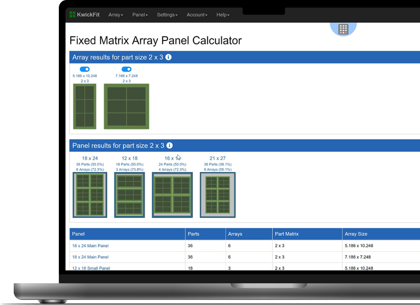
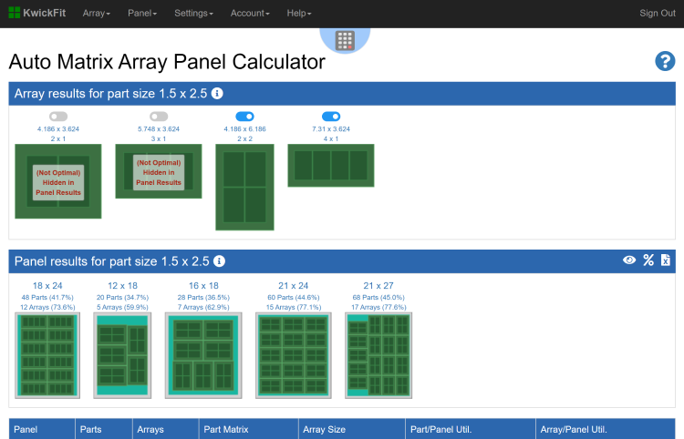
Instant What-If Analysis Discovers Real Dollar Savings.
No CAD or Gerber files. Just enter your PCB parameters and get cost-effective layouts in seconds. Test multiple configurations instantly to find cost saving optimizations on each production run.
Have questions? Contact us or check our FAQs.